Introduction
The combinational circuit does not use any memory. Hence the previous state of input
does not have any effect on the present state of the circuit. But sequential circuit
has memory so output can vary based on input. This type of circuits uses previous
input, output, clock and a memory element.
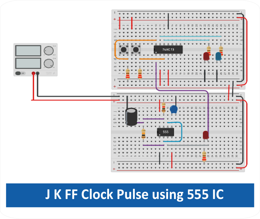
In this tutorial we will implement a sequential logic circuit called J K Flip Flop.
Objective
- To understand and implement JK Flip-Flop using universal gates.
- To design and implement a Master-Slave JK Flip-Flop using JK Flip-Flop IC.
Apparatus
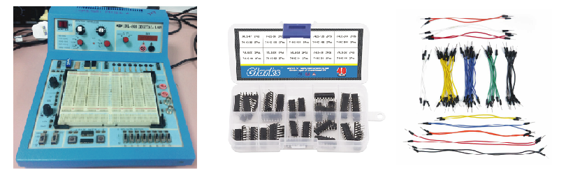
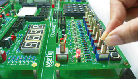
- Digital Trainer
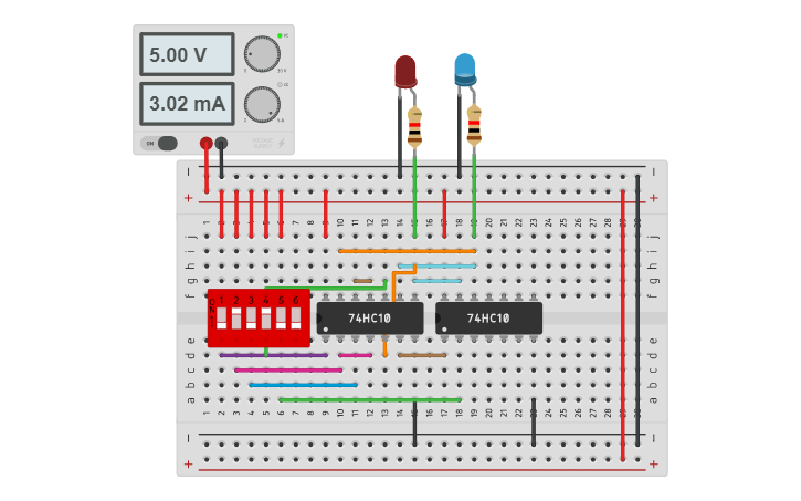
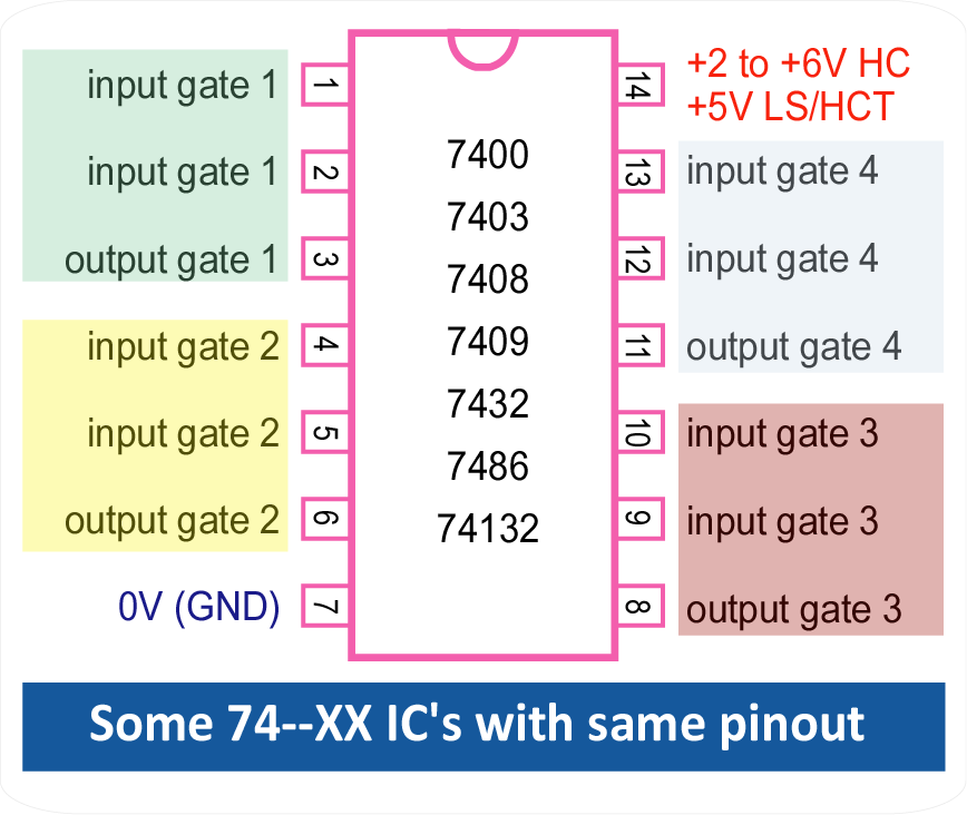
- IC's (7400, 7410, 7473 or 7476)
- Jumper Wire (M2M or as required)
- Oscilloscope (To investigate the wave shapes)
- Power Supply, Bread Board, Switches, Resistors, LEDs (When Digital Trainer Board is unavailable)
- Multimeter (Trouble Shoot purposes)
- Proteus software on your pc
Brief Theory
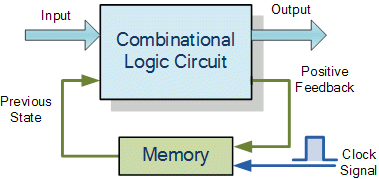
Unlike Combinational Logic circuits that change state depending upon the actual signals
being applied to their inputs at that time, Sequential Logic circuits have some form of
inherent “Memory” built in.
This means that sequential logic circuits are able to take into account their previous
input state as well as those actually present, a sort of “before” and “after” effect is
involved with sequential circuits.
In other words, the output state of a “sequential logic circuit” is a function of the
following three states, the “present input”, the “past input” and/or the “past output”.
Sequential Logic circuits remember these conditions and stay fixed in their current
state until the next clock signal changes one of the states, giving sequential
logic circuits “Memory”.
Sequential logic circuits are generally termed as two state or Bistable devices which
can have their output or outputs set in one of two basic states, a logic level “1” or
a logic level “0” and will remain “latched” (hence the name latch) indefinitely in
this current state or condition until some other input trigger pulse or signal is
applied which will cause the bistable to change its state once again.
Sequential Logic Representation
The word “Sequential” means that things happen in a “sequence”, one after another and in Sequential Logic circuits, the actual clock signal determines when things will happen next. Simple sequential logic circuits can be constructed from standard Bistable circuits such as: Flip-flops, Latches and Counters and which themselves can be made by simply connecting together universal NAND Gates and/or NOR Gates in a particular combinational way to produce the required sequential circuit.
Classification of Sequential Logic
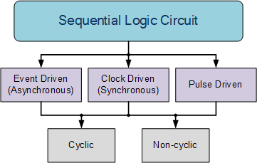
As well as the two logic states mentioned above logic level “1” and logic level “0”,
a third element is introduced that separates sequential logic circuits from their
combinational logic counterparts, namely TIME. Sequential logic circuits return back
to their original steady state once reset and sequential circuits with loops or
feedback paths are said to be “cyclic” in nature.
We now know that in sequential circuits changes occur only on the application of a
clock signal making it synchronous, otherwise the circuit is asynchronous and depends
upon an external input. To retain their current state, sequential circuits rely on
feedback and this occurs when a fraction of the output is fed back to the input and
this is demonstrated as:
Sequential Feedback Loop
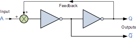
The two inverters or NOT gates are connected in series with the output at Q fed
back to the input. Unfortunately, this configuration never changes state because
the output will always be the same, either a “1” or a “0”, it is permanently set.
However, we can see how feedback works by examining the most basic sequential
logic components, called the SR flip-flop.
Flip Flop and Latches
There are two types of memory elements based on the type of triggering that is suitable to operate it.
- Latches
- Flìp Flops
Latches operate with enable signal, which is level sensitive. Whereas, flip-flops
are edge sensitive.
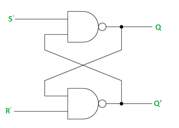
For example, let us talk about SR latch and SR flip-flops. In this circuit when you
Set S as active the output Q would be high and Q’ will be Low. This is irrespective
of anything else. (This is an active-low circuit so active here means low, but for
an active high circuit active would mean high)
A flip-flop, on the other hand, is synchronous and is also known as a gated or clocked SR latch.
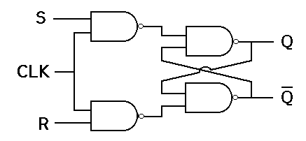
In this circuit diagram, the output is changed (i.e. the stored data is changed) only when you give an active clock signal. Otherwise, even if the S or R is active the data will not change. Let’s look at the types of flip-flops to understand better.
Types of Flip Flop
There are basically four different types of flip flops and these are:
- Set-Reset (SR) flip-flop
- JK flip-flop.
- D (Data or Delay) flip-flop.
- T (Toggle) flip-flop.
The basic S-R NAND flip-flop circuit has many advantages and uses in sequential
logic circuits but it suffers from two basic switching problems.
1. the Set = 0 and Reset = 0 condition (S = R = 0) must always be avoided
2. if Set or Reset change state while the enable (EN) input is high the
correct latching action may not occur
Then to overcome these two fundamental design problems with the SR flip-flop design,
the JK flip Flop was developed.
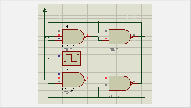
J K Flip Flop
This simple JK flip Flop is the most widely used of all the flip-flop designs and is
considered to be a universal flip-flop circuit. The two inputs labelled “J” and “K”
are not shortened abbreviated letters of other words, such as “S” for Set and “R”
for Reset, but are themselves autonomous letters chosen by its inventor Jack Kilby
to distinguish the flip-flop design from other types.
The sequential operation of the JK flip flop is exactly the same as for the previous
SR flip-flop with the same “Set” and “Reset” inputs. The difference this time is that
the “JK flip flop” has no invalid or forbidden input states of the SR Latch even when
S and R are both at logic “1”.
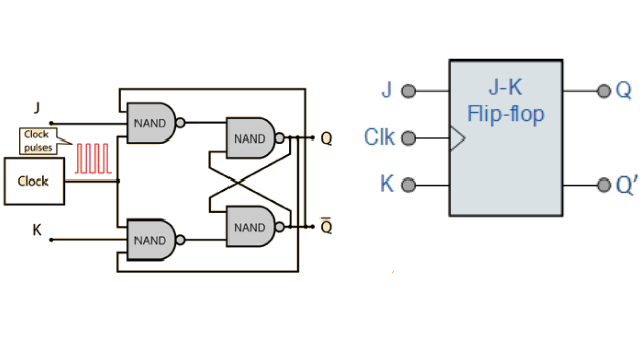
The JK flip flop is basically a gated SR flip-flop with the addition of a clock input
circuitry that prevents the illegal or invalid output condition that can occur when
both inputs S and R are equal to logic level “1”. Due to this additional clocked
input, a JK flip-flop has four possible input combinations, “logic 1”, “logic 0”,
“no change” and “toggle”. The symbol for a JK flip flop is similar to that of an
SR Bistable Latch as seen in the previous tutorial except for the addition of a
clock input.
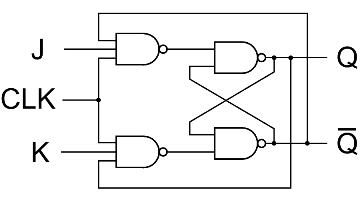
The Basic JK Flip-flop
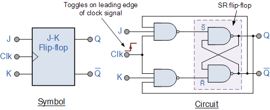
Both the S and the R inputs of the previous SR bistable have now been replaced by two
inputs called the J and K inputs, respectively after its inventor Jack Kilby. Then
this equates to: J = S and K = R.
The two 2-input AND gates of the gated SR bistable have now been replaced by two
3-input NAND gates with the third input of each gate connected to the outputs at
Q and Q. This cross coupling of the SR flip-flop allows the previously invalid
condition of S = “1” and R = “1” state to be used to produce a “toggle action”
as the two inputs are now interlocked.
If the circuit is now “SET” the J input is inhibited by the “0” status of Q through
the lower NAND gate. If the circuit is “RESET” the K input is inhibited by the “0”
status of Q through the upper NAND gate. As Q and Q are always different we can use
them to control the input. When both inputs J and K are equal to logic “1”, the JK
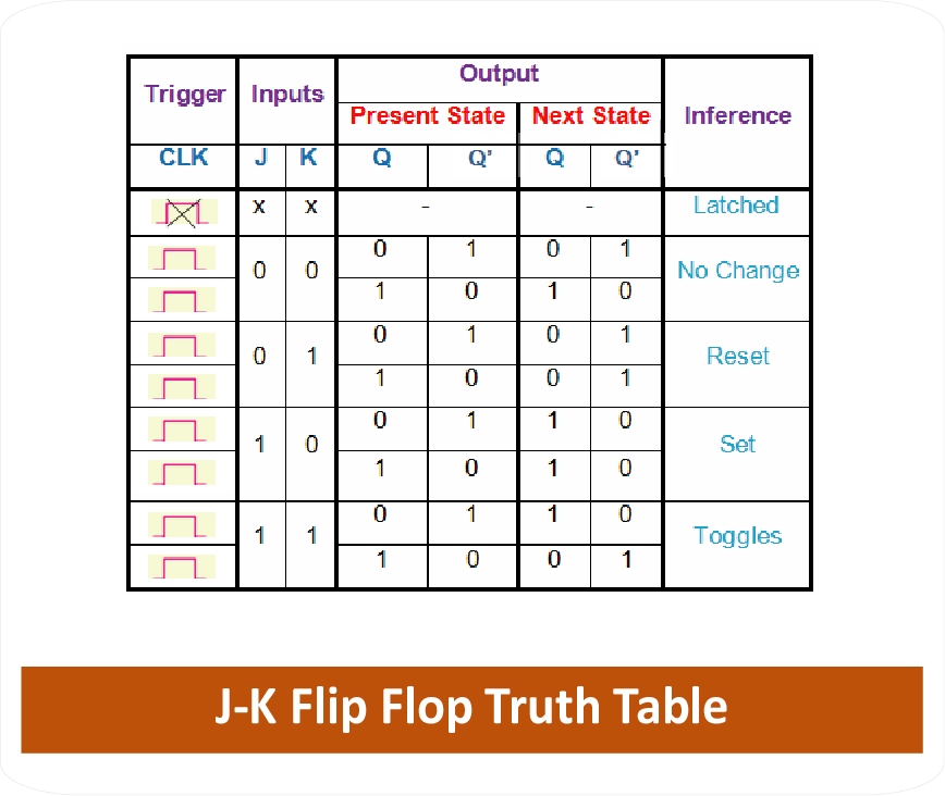
flip flop toggles as shown in the following truth table.
The Truth Table for the JK Function
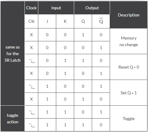
Then the JK flip-flop is basically an SR flip flop with feedback which enables only
one of its two input terminals, either SET or RESET to be active at any one time
under normal switching thereby eliminating the invalid condition seen previously
in the SR flip flop circuit.
However, if both the J and K inputs are HIGH at logic “1” (J = K = 1), when the clock
input goes HIGH, the circuit will “toggle” as its outputs switch and change state
complementing each other. This results in the JK flip-flop acting more like a T-type
toggle flip-flop when both terminals are “HIGH”. However, as the outputs are fed back
to the inputs, this can cause the output at Q to oscillate between SET and RESET
continuously after being complemented once.
While this JK flip-flop circuit is an improvement on the clocked SR flip-flop it also
suffers from timing problems called “race” if the output Q changes state before the
timing pulse of the clock input has time to go “OFF”. To avoid this the timing pulse
period ( T ) must be kept as short as possible (high frequency). As this is sometimes
not possible with basic JK flip-flops built using basic NAND or NOR gates, far more
advanced master-slave (edge-triggered) flip-flops were developed which are more stable.
Master-Slave JK Flip-flop
The master-slave flip-flop eliminates all the timing problems by using two SR flip-flops
connected together in a series configuration. One flip-flop acts as the “Master” circuit,
which triggers on the leading edge of the clock pulse while the other acts as the “Slave”
circuit, which triggers on the falling edge of the clock pulse. This results in the two
sections, the master section and the slave section being enabled during opposite half-cycles
of the clock signal.
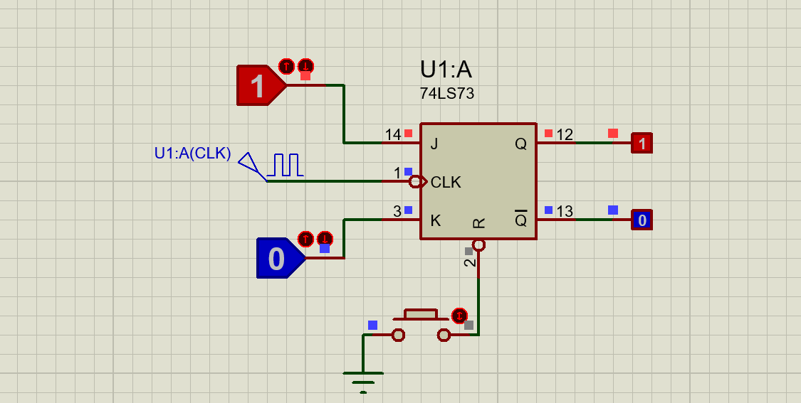
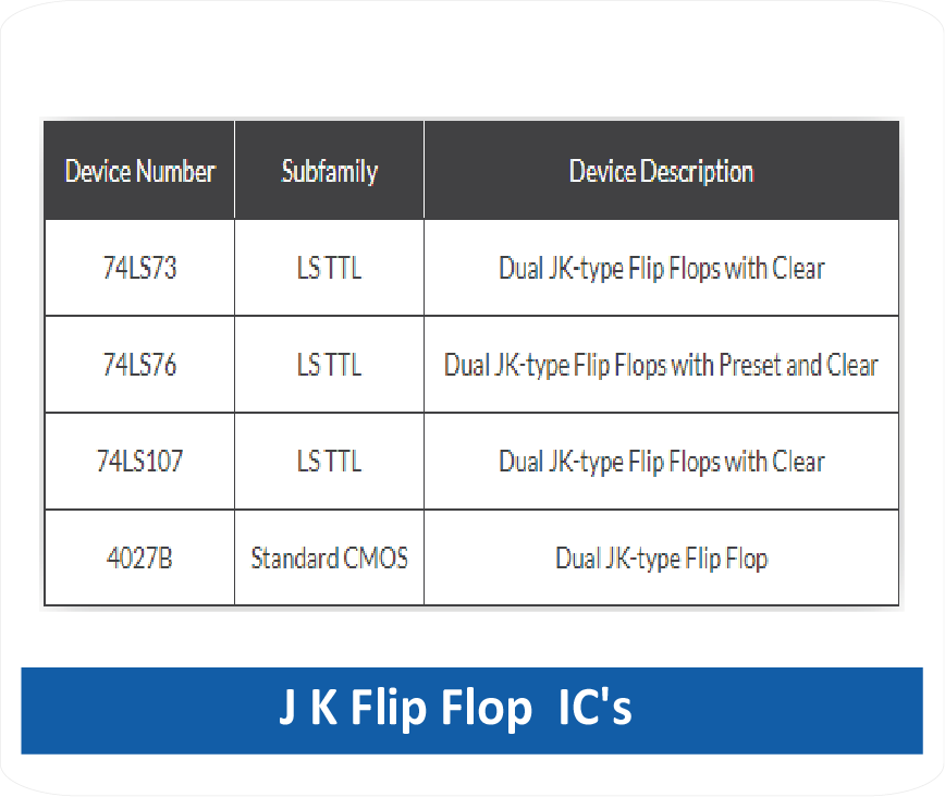
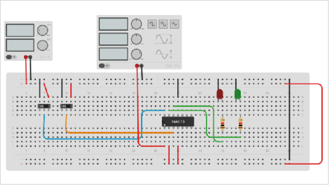
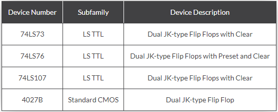
The TTL 74LS73 is a Dual JK flip-flop IC, which contains two individual JK type bistable’s
within a single chip enabling single or master-slave toggle flip-flops to be made. Other JK
flip flop IC’s include the 74LS107 Dual JK flip-flop with clear, the 74LS109 Dual positive-edge
triggered JK flip flop and the 74LS112 Dual negative-edge triggered flip-flop with both preset
and clear inputs.
Dual JK Flip-flop 74LS73
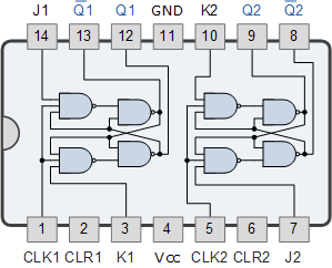
Other Popular JK Flip-flop ICs
The Master-Slave Flip-Flop is basically two gated SR flip-flops connected together in a series configuration with the slave having an inverted clock pulse. The outputs from Q and Q from the “Slave” flip-flop are fed back to the inputs of the “Master” with the outputs of the “Master” flip flop being connected to the two inputs of the “Slave” flip flop. This feedback configuration from the slave’s output to the master’s input gives the characteristic toggle of the JK flip flop as shown below.
The Master-Slave JK Flip Flop
The input signals J and K are connected to the gated “master” SR flip flop which “locks”
the input condition while the clock (Clk) input is “HIGH” at logic level “1”. As the clock
input of the “slave” flip flop is the inverse (complement) of the “master” clock input,
the “slave” SR flip flop does not toggle. The outputs from the “master” flip flop are
only “seen” by the gated “slave” flip flop when the clock input goes “LOW” to logic level “0”.
When the clock is “LOW”, the outputs from the “master” flip flop are latched and any
additional changes to its inputs are ignored. The gated “slave” flip flop now responds to
the state of its inputs passed over by the “master” section.
Then on the “Low-to-High” transition of the clock pulse the inputs of the “master” flip flop
are fed through to the gated inputs of the “slave” flip flop and on the “High-to-Low” transition
the same inputs are reflected on the output of the “slave” making this type of flip flop edge
or pulse-triggered.
Then, the circuit accepts input data when the clock signal is “HIGH”, and passes the data to
the output on the falling-edge of the clock signal. In other words, the Master-Slave JK Flip
flop is a “Synchronous” device as it only passes data with the timing of the clock signal.
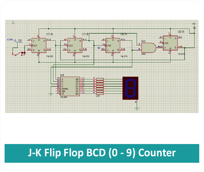
In the next tutorial about Sequential Logic Circuits, we will look at johnson Counter and
Ring Counter circuits.
Applications of Flip-Flops
- Counters
- Frequency Dividers
- Shift Registers
- Storage Registers